Programator Atmel At89c2051
AN_3554 - Migrating from AT89C2051/C4051 to AT89S2051/S4051. AN_3573 - Migrating from AT89C2051/C4051 to AT89LP2052/LP4052. NXP Flash MCU to. I am a newbie with ATMEL MCU family. But i want to change the software on a AT89C2051 wich contains an 'HORLOGE 7 segm.
If I set up any compatibility mode, the software read out nothing, so I got 00FF 00FF 00FF 00FF. And if I dont set up any compatibility mode, all the read out files will be different! But may be the same just slip the code anyway! Added after 1 hours 12 minutes: Is it a problem, that there is only 11,26V on the RST pin while the programming is running??? Added after 30 minutes: I read the 89c2051 datasheet, and I read this: When the power is on, there must be 5V on the rst pin, and when the programming starts, there must be 12v! But when I power on my device, there is 3,34V on the rst pin, and when I start the programming, ther is 11,26V.
Is it normal??? The voltage applied on RST pin at power up must be greater than 0,7Vcc, that is greater than 3,5v You should get 4,2 - 4,3v (like with +12v, that drops to 11,3v).
11,3v on RST pin during programming will violate the specs but it still works for me. Download the parallel port tester from here: and check the hardware as follows. At least you will know that your problems are due to the software and not from hardware. It's really madness and a lot of peoples could claims it would be better to switch to another micro upload through ISP with the same program (I call AT89S52). Well, it will not fit on the keyboard logger wires due to his size (DIP 40 or PLCC 44). Nevertheless, if you can convert the assembler code from 8051 to your favorite AVR, then all the things bellow are useless.
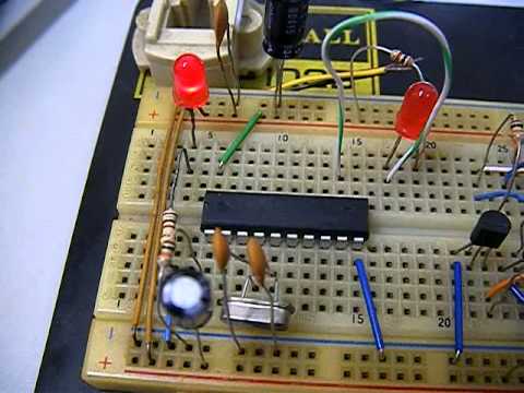
All pins are from DB25 plug. Push C0 Pin 1 turn yellow 2. Push C1 Pin 14 turn yellow 3. Thus the RST pin voltage drops to 0v (insert now the micro in socket and aply the power supply) 4. Spiderman 3 pc game sound files free. Push D7 Pin 9 turn green 5.
Thus data in the storage register of 4094 appears at the outputs. Push D6 Pin 8 turn green (D6 is pushed in the first shift register) 7. Push D6 Pin 8 turn off 8. Repeat steps 6-7 five times more, for the next five '0' load into shift register 9. Push D5 Pin 7 turn green (set data '1') 10.
Push D6 Pin 8 turn green (clock in) (P3.2 pin must be kept at high level) 11. Push D6 Pin 8 turn off 12.
Push D5 Pin 7 turn off (set data '0') (the XTAL1 is at low level in order to reset the address counter of 89C2051) 13. Push D6 Pin 8 turn green (clock in) 14. Push D6 Pin 8 turn off 15. Push D4 Pin 6 turn green (set strobe, that is data in each shift register is transffered to the storage register 16.
Push D4 Pin 6 turn off 17. Push C1 Pin 14 turn off (pin RST goes to +5v) Now you must be able to see the low nibble of the first signature byte 1110 It will appear on the status register as follows: S4 blue lit pin 13 S5 blue lit pin 12 S7 off pin 11 (pin 11 is hardware inverted, that's why appears off, even if is '1') S6 off pin 10 18. Push C2 Pin 16 turn yellow (on the status register appears the high nibble of the first signature byte 0001 S4 off pin 13 S5 off pin 12 S7 blue lit pin 11 (pin 11 is hardware inverted, that's why appears lit, even if is '0') S6 blue lit pin 10 19. Push C2 Pin 16 turn off 20. Push D6 Pin 8 turn green (D6 is pushed in the first shift register) 21. Push D6 Pin 8 turn off 22. Repeat steps 20-21 five times more, for the next five '0' load into shift register 23.
Push D5 Pin 7 turn green (set data '1') 24. Push D6 Pin 8 turn green (clock in) (P3.2 pin must be kept at high level) 25. Push D6 Pin 8 turn off 26. Push D6 Pin 8 turn green (clock in) (the XTAL1 pin will raise to +5v after strobe) 27. Push D6 Pin 8 turn off 28. Push D5 Pin 7 turn off (reset data) 29.